Photonic Processors: How Computing on Light Speeds Up AI Inference (2025)
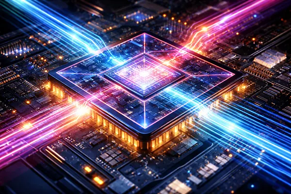
Photonic processors are no longer a purely academic curiosity. By 2025, several companies and research groups have demonstrated that light can handle parts of the maths behind neural networks faster and with less energy than purely electronic approaches—especially for the matrix multiplications that dominate inference. The key idea is simple: instead of pushing electrons through transistors to multiply and accumulate numbers, you encode values into light and let optical interference perform the heavy lifting. What makes this practical today is the surrounding ecosystem: mature silicon photonics, improved packaging, optical interconnect chiplets, and a clearer understanding of where photonics actually beats GPUs and where it does not.
Why light can outperform electrons for inference workloads
Most modern AI inference—whether it is a language model producing tokens or a vision model classifying images—boils down to linear algebra. In practice, that means large matrix multiplications repeated millions of times. Photonics is naturally good at this because interference and phase shifts can represent multiply-and-accumulate operations in parallel. Instead of executing each multiply electronically, an optical circuit can apply many “weights” at once as a beam passes through a mesh of interferometers. The result is not magic; it is physics doing analogue computation at extremely high bandwidth.
This physics advantage shows up in two places that matter to operators: throughput and energy per operation. Optical signals can propagate and mix at very high effective rates, and—crucially—moving information with light often costs less energy than moving it through long copper traces at the same bandwidth. That is why the photonics story in 2025 is closely tied to data movement: even when the compute is hybrid (optical + electronic), cutting the cost of shuttling activations and weights can materially improve inference efficiency in a rack.
However, the benefit is workload-dependent. Photonic compute is strongest when the job is dominated by dense linear layers and when the system can keep the optical core fed with data. If the model spends a lot of time in non-linear functions, sparse operations, branching logic, or frequent precision conversions, the gains can shrink quickly because electronics still has to manage control flow and clean up the results.
How photonic matrix multiplication actually works
Many photonic AI engines rely on Mach–Zehnder interferometer (MZI) meshes. In plain terms, an MZI can act like a tunable “knob” that changes how two light paths combine. Arrange thousands of these knobs into a mesh and you can implement a matrix transform: inputs are encoded into light intensities or phases, the mesh applies the weight matrix through interference, and detectors read the output back into electronics. This is why you often see photonic compute described as analogue: the physics represents continuous values, even if the surrounding digital system treats them as numbers.
Because the optical part is analogue, calibration matters. Temperature drift, fabrication tolerances, and laser stability all affect accuracy. In 2025 systems, this is typically handled with feedback loops, periodic recalibration, and mixed-precision strategies—using photonics for the bulk multiply and electronics for compensation, scaling, and error control. This is not a weakness so much as an engineering reality: you trade some complexity in calibration to reduce the fundamental energy cost of the core linear algebra.
Another practical point is precision. Photonic compute is often most attractive for inference at reduced precision (for example, formats comparable to 8-bit or lower in effective accuracy) because many deployed models tolerate quantisation. The industry trend toward quantised inference helps photonics: if your production stack is already tuned for efficient, slightly noisy arithmetic, photonic accelerators can slot into that philosophy more naturally than when everything demanded strict floating-point behaviour.
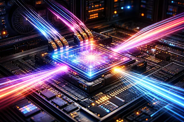
What “real” photonic processors look like in 2025
The most useful way to understand 2025 photonics is to separate two categories: (1) photonic compute engines that perform parts of the neural network maths using light, and (2) optical interconnect technology that moves data between chips using light. Both can accelerate inference, but they do so in different ways. Compute engines aim to reduce the energy and time spent on matrix operations. Optical interconnect aims to reduce the energy and latency of moving tensors between GPUs, memory, and accelerators—often the hidden bottleneck in scaled inference deployments.
On the compute side, Lightmatter has positioned Envise as a photonic computing system designed for AI workloads, explicitly targeting performance and energy efficiency. The company markets Envise as a photonic computing product for neural networks, which signals that photonics is being packaged as a deployable system rather than a lab demo.
On the interconnect side, optical chiplets are becoming a serious theme. Ayar Labs, for example, has announced a UCIe optical chiplet approach intended for AI scale-up architectures, aiming to keep accelerators communicating at very high bandwidth across distances that would be painful for copper at similar power levels. In practice, that can translate into better utilisation: less time waiting for data, more time doing inference.
Interconnect-first photonics: getting inference systems to scale
Large inference clusters are increasingly constrained by data movement. As models grow, you often need model parallelism, tensor parallelism, or pipeline parallelism—even for inference—because the weights no longer fit neatly on a single device. That makes the “fabric” between devices a first-class performance limiter. Optical links can help because they can deliver high bandwidth at lower loss over distance, and they avoid some of the signal integrity headaches that appear when pushing copper to extremes.
Ayar Labs’ optical I/O direction is designed around integration into chiplet ecosystems, which matters because the industry is standardising around chiplet-based packaging. Their messaging in 2025 focuses on optical I/O chiplets for AI scale-up, a sign that photonics is being aimed at mainstream system architectures rather than niche bespoke machines.
Lightmatter has also highlighted photonic interconnect with products like Passage, including announcements around the Passage M1000 and related components intended for very high-speed chip-to-chip links. The reason this matters for inference is straightforward: once the model is sharded across devices, your effective tokens-per-second can become a networking problem as much as a compute problem.
Deployment realities: costs, toolchains, and where photonics fits best
For most teams, the hard question is not “Is photonics fast?” but “Where does it pay off?” In 2025, photonic accelerators are most convincing in scenarios where inference is dominated by dense linear layers, where energy cost is a primary constraint (for example, datacentres hitting power ceilings), and where the operator can keep utilisation high. If a photonic core sits idle waiting for data or spends too much time converting between representations, the theoretical physics advantage turns into an expensive science project.
Toolchains are improving, but they are still a consideration. Photonic compute often requires mapping neural network layers to optical meshes, managing quantisation strategies, and handling calibration. That means the software stack has to expose the right abstractions: a compiler that knows how to schedule optical GEMMs (matrix multiplications), runtime support for calibration, and clear performance models so engineers can predict when a layer should run optically versus electronically. Organisations that already invest heavily in inference optimisation—quantisation, kernel fusion, memory planning—are typically best positioned to evaluate photonics properly.
There is also a hybrid future. Many “photonic” systems are not purely optical computers; they are mixed systems. Electronics still handles control, non-linearities, memory addressing, and parts of the accumulation pipeline. In practice, the likely near-term pattern is that photonics accelerates the heaviest linear algebra, while advanced packaging and optical I/O reduce the cost of moving data around a multi-chip system.
Practical decision checklist for engineers in 2025
First, quantify whether your inference workload is truly matrix-bound. If your profiling shows that most time and energy is spent in dense GEMMs and memory traffic that feeds them, photonic approaches are worth examining. If instead the workload is dominated by attention overhead, irregular memory access, routing logic, or significant post-processing, you may see limited benefit from an optical compute core—even if optical links still help at cluster scale.
Second, evaluate integration risk. Photonic compute introduces calibration and environmental sensitivity, so you need a plan for monitoring and maintenance. If your datacentre operations can support periodic calibration cycles and you have a clear reliability story, photonics becomes more realistic. Research and industry coverage in 2025 repeatedly highlights that scalable, sustainable AI hardware is tied to photonic integrated circuits, but the engineering burden is non-trivial.
Third, consider the interconnect path even if you do not adopt photonic compute immediately. Optical I/O chiplets and silicon photonics for links can deliver tangible benefits by reducing the energy and latency of data movement. Intel, for example, has been public about advances in silicon photonics for high-bandwidth optical interconnect building blocks, reflecting how much attention the industry is placing on optical connectivity as AI systems scale.